2012-03-14

No.10


본 정부는 전기자동차 분야에서 일본의 우위성과 한국 등 외국의 추격사례를 분석하고 이에 대한 국가적인 개발정책을 수립하고 있다. 유럽과 미국의 완성차 제조업체들은 복수의 전지 제조업체와 제휴관계를 맺고 있다. 미국과 중국의 신흥기업은 휴대형 전자기기용 리튬이온 이차전지를 탑재한 전기자동차를 시판하고 있다.                                                                                           
나라별 개발 계획             
국내 개발계획              
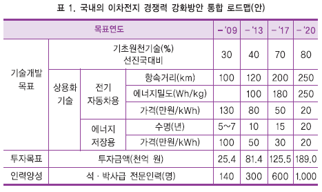
지식경제부, 기획재정부, 교육과학기술부 및 녹색성장위원회는 제8차 녹색성장위원회 보고회(2010.7)에서 “이차전지경쟁력 강화방안”을 보고한 바 있다. 세계적 경쟁력을 갖춘 소형전지는 시장에 맡기되 정부는 중대형 전지제조 및 소재 산업에 지원 역량을 집중하기 위해 표 1과 같은 통합로드맵(안)을 제시했다.


▶ 중대형 전지 경쟁력 강화
▶ 이차전지 핵심소재 산업육성
▶ 선 순환적 산업생태계 구축
▶ 범국가적 이차전지 산업 통합로드맵 추진 등의 4대 정책과제를
   제시하고 범 정부차원에서 추진해 나갈 계획을 밝혔다.

일본 정부의 개발계획         
  
가. 일본 정부의 전기자동차 관련 우위성 분석    


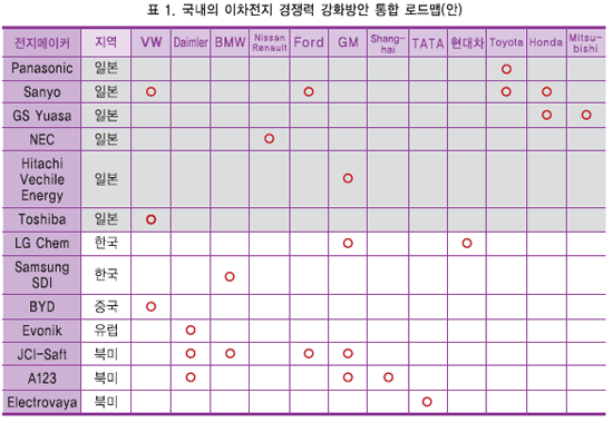
일본 정부는 전기자동차 분야에서 일본의 우위성과 한국 등 외국의 추격사례를 분석하고 이에 대한 국가적인 개발정책을 수립하고 있다. 표 2는 전지 제조업체와 완성차 제조업체와의 제휴관계를 정리한 것이다. 유럽과 미국의 완성차 제조업체들은 복수의 전지 제조업체와 제휴관계를 맺고 있음을 알 수 있다.
일본 완성차 제조업체의 기술적 우위를 추격하기 위하여 수평 분업화로 여러 이차전지 제조업체와 연계하면서 개발을 가속화시키고 있다. 또한 미국과 중국의 신흥기업은 휴대형 전자기기용 리튬이온 이차전지를 탑재한 전기자동차를 시판하고 있다.

나. 일본 정부의 자동차용 축전기술 개발      
자동차용 축전장치 개발은 연료전지 자동차용 리튬이온 이차전지기술 개발(2002.4~2006.3), 차세대 자동차용 고성능 축전시스템기술 개발(Li-EAD)(2007.4~2012.3), 혁신 축전지 첨단과학 기초연구사업(RISING)(2009.4~2015.3)의 3단계로 구성되어 추진되고 있다. 혁신 축전지 첨단과학 기초연구사업에는 약 210억 엔의 예산이 투입된다. 차세대 자동차용 고성능 축전시스템기술 개발은 리튬이온 이차전지 등의 재료와 모듈 등의 요소기술 개발, 혁신적인 성능 향상, 저가격화, 안전성 향상에 이어지는 양극소재 등을 개발하는 차세대 기술개발, 그리고 축전지의 수명 예측, 내구성, 안전성시험방법의 확립과 규격화, 반응기구의 해석기법 등의 기반을 구축하기 위한 기술개발로 구성되어 있다. 요소기술 개발과제(전지 구성재료 개발)의 성능목표는 에너지밀도 200Wh/kg 이상, 출력밀도 2,500W/kg 이상, 비용 3만 엔/kWh 이하의 전망을 얻는 것이다. 요소기술 개발과제(전지개발)의 성능목표는 에너지밀도 100Wh/kg, 출력밀도 2,000W/kg, 수명 10년 이상, 비용 414만 엔 이하이다. 차세대기술 개발과제의 성능목표는 500Wh/kg 이상이고 혁신형 축전지 개발과제의 성능목표는 700Wh/kg, 출력 밀도 1,000W/kg을 실현시키는 것이다.
2010년 3월까지 요소기술 과제로 18건, 차세대기술 개발과 제로 30건, 기반기술 과제로 1건이 채택되어 시행되었다. 2010년 4월부터는 첨단 리튬전지계통이 8건, 금속-공기계통 3건, 유환계 2건, poly-cation계 2건, 해석기술 등 차세대 기술개발 과제에서 27건이 수행되고 있다. 요소기술 개발과제로는 모듈 개발 3건, 재료 개발 7건, 모터 개발 5건 등이 실시되고 있다.
2009년도 주요 연구 성과로는 「이론용량을 초월한 산화주석음극소재 개발」, 「1,000사이클 이상을 달성한 실리콘계 음극소재」, 「고전압, 고안전성 축전지를 실현하는 불소계 전해액개발」,「희토류 금속 사용량을 반감할 수 있는 고출력 밀도모터의 개발」등이 있다.
다. 저탄소형 고용 창출산업 입지 추진 사업비  보조금사업    
일본 정부도 미국정부의 고용 창출을 위한 ARRA 프로젝트와 유사한 ‘저탄소형 고용 창출산업 입지추진 사업비 보조금’ 사업을 운용하고 있다. 성장 잠재력이 큰 시장에서 신뢰성이 높은 기술력을 갖는 등 국제경쟁력이 큰 기업의 해외 유출을 막으면서 일본 국내의 고용 창출과 지역경제 활성화를 위하여 정부가 보조금을 지급하는 제도이다. 2010년도에는 예산총액 297억 엔으로 42개 기업이 채택되었다. 채택된 기업 가운데 리튬이온 이차전지용 양극소재 제조공장에 대하여 최대 50억 엔의 보조금이 지급되는 Lithium Energy Japan 등 리튬이온 이차전지 관련 기업과 전기자동차 관련 기업은 다음과 같다.
① 리튬이온 이차전지 관련 보조금 지급(18개 기업): Sony Energy Device(휴대전화 기지국용 전원 등의 리튬이온 이차전지 제조), Hitachi Vehicle Energy(상용차용 리튬이온 이차전지 제조), NEC Tokin(전력저장용 리튬이온 이차전지와 전극의 제조), Toshiba(전력저장용 등 리튬이온 이차전지 제조), Nagano Automaton(리튬이온 이차전지 관련 장치의 제조), Enax(전력저장용 등 리튬이온 이차전지 제조), Tanaka Chemical Research Lab.(리튬이온 이차전지 양극소재 제조), Lithium Energy Japan(일반 자동차용 리튬이온 이차전지 제조), Asahi Kasei e-Materials(리튬이온 이차전지용 분리막 제조), Shin Kobe Denki(산업용 등 리튬이온 이차전지의 제조), Sanyo Denki(일반 자동차용/전력저장용 리튬이온 이차전지 제조), Umikoa Japan(리튬이온 이차전지 양극소재 제조), Fuji Hatcho(리튬이온 이차전지 케이스와 덮게 제조), Toda Kogyo(리튬이온 이차전지 양극소재 제조), Titan Kogyo(리튬이온 이차전지 관련 부재 제조), Ube Kosan(리튬이온 이차전지 분리막과 전해액 제조), Central Glass(리튬이온 이차전지 전해액 제조), Mitsubishi(리튬이온 이차전지의 관련부재 제조), Nippon Advanced Paper Industry(리튬이온 이차전지 분리막 제조) 등.
② 전기자동차 관련 보조금 지급(5개 기업): Kofu Meidensha(전기자동차용 모터 제조), Tamagawa Seiki(전기자동차용 모터제어장치 제조, Meidensha(전지가동차용 인버터 제조),
Nichicon(전기자동차용 충전기 제조), Nippon Ceramics(전기 자동차용 모터 제어장치 제조).
Mitsubishi ‘iMiEV’ - 용량이 6kWh이고 항속거리가 160km인 MiEV는 Mitsubishi Auto와 GS Yuasa가 합작하여 설립한 Lithium Energy Japan이 제조한 리튬이온 이차전지를 탑재한다. 2009년 6월 2일부터 Kusazu 공장에서 연간 20만 셀(iMiEV 2,300대분)을 생산하고 있다. Kyoto 사업소 등의 추가로 최종적으로는 600만 셀(자동차 10만 대분)의 공급체제를 구축할 계획이다.
미국 정부의 개발계획          
미국 정부의 전기자동차 개발계획은 3가지 형태로 추진되고 있다. ① 전기자동차 용 축전장치 기술개발과 주행 모터/인버터 등 전기자동차 주행시스템 등의 기술개발 ② ARRA 프로젝트의 자금에 의한 이차전지 등 생산거점의 미국 내 건조 ③ AVTM(Advance Vehicle Technology Manufacturing loan Program)에 의한 전기자동차 등 환경친화형 자동차의 생산거점을 미국 내에 건설하는 프로그램.
가. 전기자동차용 축전장치 등 요소기술 개발        
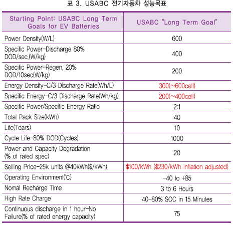
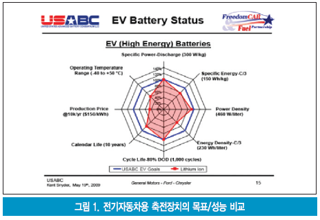
표 3과 그림 1은 미국 USABC의 전기자동차용 축전장치의 성능목표와 현재의 목표/성능을 비교하고 있다.


나. 전기자동차용 요소부품의 생산거점을 미국 내 건조     
미국은 정부와 민간이 힘을 합쳐 생산체제 구축을 가속시키고 있다. 리튬이온 이차전지의 생산거점은 일본과 한국 그리고 중국 등 아시아지역에 집중되어 있어 미국에는 국제경쟁력 있는 리튬이온 이차전지 제조업체가 없었다. 미국 오바마 정부는 환경친화형 자동차의 핵심기술인 축전장치 등 관련 요소기술의 생산시설을 미국에 구축하여 자동차 산업의 국제경쟁력을 향상시키고 고용을 창출하는 등 경기 자극책으로 ARRA법을 활용한 대규모 지원계획을 발표하였다. 이 사업에 선정되어 미국 내에 생산시설을 구축하는 기업을 그림 2와 같다.


이 자금은 매칭펀드(maching fund) 방식이다. 기업이 동등한 금액을 출자하여 생산기설을 구축하기 때문에 생산 설비 투자액은 2배가 된다.

다. 환경친화형 자동차 제조시설의 미국 내 건조         
미국 정부는 기술 집약과 경쟁 촉진정책을 통해 석유 공급의 해외의존도를 낮추어 소비자 지출을 저감하고 첨단 자동차 개발과 생산기술에서 세계를 선도하며 고품질의 고용을 확보할 목적으로 자동차 분야에서 미국 내에 생산시설을 건조하는 5개 프로젝트를 선정하였다. 총액 85.91억 달러의 융자계획을 발표하고 Nissan에 14.5억 달러, Tesla Motors에 4.65억 달러, Ford Motor에 59.37억 달러를 융자하는 등 3개사에 저리융자를 실시하였고, Fisker Automotive에 5.29억 달러, Tenneco에 2,400만 달러를 융자하였다.
Nissan LEAF : Oppama 공장의 LEAF 생산용량은 연간 5만 대이다. 내연기관 자동차 생산라인과 혼합하여 생산하며 휘발유 탱크 장착공정에서 전지 팩을 장착하고 엔진 장착공정에서 모터/인버터 모듈을 장착한다. 2010년 10월 22일부터 생산을 개시했다. 2010년 12월에는 일본과 미국에서, 2011년 초에는 유럽에서 판매한다. 이를 위해서 11월부터 미국에 수출하고 12월에는 유럽으로 수출한다. 2012년 후반부터 미국 Smyner 공장, 2013년에는 영국의 Suntherland 공장에서도 생산한다. Smyra의 생산규모는 연간 15만 대이며, Suntherland는 연간 5만 대이다. Oppama 공장은 이들의 모공장(mother plant)이 되며 축적된 노하우와 성과를 일본 외의 EV 생산거점에 이식하게 된다.
Nissan의 보급전략 : 정부 보조금을 활용하여 내연기관 자동차가격과 비슷한 수준으로 판매할 계획이다. 이차전지 팩의 리스판매를 구상하고 있다. 자동차가격을 200만 엔, 이차전지 팩 가격을 200만엔으로 가정하고 있으며, 소비자는 200만 엔만 지불하고 전기자동차를 구매하게 된다. 연간 주행거리를 6,000km로 가정하면 연비 10km/리터로서 600리터의 휘발유가 필요하다. 휘발유가격을 130/리터로 하면 연간 7만 8,000엔이 소요된다. kWh당 주행거리를 6KM로 가정하면 전기소비량은 연간 1,000kWh이며, 이를 야간의 전력으로 충전하면 비용이 1만엔이기 때문에 이차전지 팩의 리스가격이 6만 8,000엔이면 종합적인 유지비가 같아지게 된다. 10년 후의 잔존용량은 80% 가량이며 열화에 의한 감손액은 40만 엔이 되어 연간 4만 엔이 된다. 리스가격은 실현 가능한 수준이다. 따라서 10년 사용 후의 이차전지 팩을 재생에너지나 백업용 축전지로 재사용하면 가격경쟁력이 충분하다. 현재 이차전지 팩은 자동차와 일체로 취급되고 있어 분리하여 리스를 못하게 하고 있으나 앞으로는 이를 해제하는 것도 가능할 것이다.
Tesla의 Model S : 미국 정부의 지원금 4.65억 달러 중에서 3.65억 달러는 Southern California에 Model S 생산 공장을 건설하는 데 사용된다. 2013년까지 연간 생산량 20,000대이다. 전기자동차의 기본가격은 57,000달러이며 세금공제 등으로 구입가격은 49,000달러가 될 것으로 전망하고 있다. 항속거리가 260/370/480km인 3종류의 자동차를 생산한다. 나머지 1억 달러는 이차전지 팩과 전동 동력장치 생산시설의 건설에 사용된다. 2011년 초에는 시범 생산이 시작되며 2012년까지 10,000팩, 2013년에는 30,000팩의 생산능력을 갖게 된다. 여기서 생산된 팩은 Tesla 이외의 완성차 제조업체에게도 판매된다.
현시점에서는 Panasonic Energy의 18650형 니켈계 양극 고용량 휴대형 전자기기용 리튬이온 이차전지 팩을 약 4,000개 제작하고 있다. Panasonic Energy는 2010년 3월 25일에 일본 Osaka Sumie지구에 연산 3억 개의 셀 생산시설을 준공한 바 있다. 이 공장은 극판 제조로부터 셀 제조까지의 일관 생산라인이며 자동차용과 가정용 재생에너지 축전장치 및 백업 전원을 공급할 예정이다. 2010년 4월부터 월 1,000만개의 셀을 생산하고 있다. 이와는 별도로 Panasonic은 3.6V 리튬이온 이차전지 7개를 직렬로 연결하여 25.2V를 실현하고 이것을 20개 병렬로 연결하여 모두 140개의 셀로서 1.5kWh 모듈을 개발하여 시판하고 있다.

라. Ford의 전기자동차 Focus Electric    
항속거리는 160km이다. Michigan주에서 생산하고 2011년 말에는 미국, 2012년에는 유럽에서 판매한다. Ford는 2013년까지 미국과 유럽에서 5개 차종의 전동차량(EV/HEV/PHEV)을 판매할 계획이며 Focus Electric은 그 중의 하나이다. 미국 시장에 투입할 Focus Electric에는 LG화학의 미국 자회사 Compact Power로부터 전지 팩을 공급받는다.


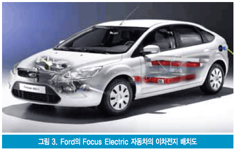
현재 미국에서 시험주행 중에 있는 Focus EV에는 한국 Kokam의 리튬이온 이차전지가 탑재되어 있는 것으로 알려져 있다.
중국 정부의 개발계획          
중국 정부의 전동자동차 개발계획은 매우 의욕적이다. 2010년 말까지 30kWh의 전지 팩을 탑재하여 항속거리 200km인 전기자동차를 15만 대 보급시킬 계획이다. 또한 2015년까지는 수백만 대, 2020년까지는 수천만 대 규모로 확대할 방침이다. 이를 위한 축전장치는 2009년 현재 중국 내 생산용량이 900GWh이지만 2020년까지 4,000GWh로 높일 방침이다. 리튬이온 이차전지가격은 현재 1Wh당 4.5위안인 것을 1.5위 안으로 내리고 에너지밀도는 현재의 80Wh/kg을 120Wh/kg까지 향상시킨다. 2020년에는 전기자동차의 항속거리를 100~250km로 하고, 플러그인 하이브리드자동차의 전기주행거리를 50~70km로 하며, 에너지밀도를 250Wh/kg으로 높이고 추가적으로 400Wh/kg을 실현할 수 있는 새로운 재료를 개발한다. 출력밀도는 5,000W/kg을 목표로 한다.
개량형 리튬이온 이차전지     
일본의 리튬이온 이차전지 가격 저감 시나리오         
일본 신에너지·산업기술총합연구기구(NEDO)의 로드맵에서는 2009년 시점에서 15만 엔/kWh로 추정되는 전기자동차용 이차전지가격을 2010년에는 10만 엔/kWh, 2015년에는 3만 엔/kWh, 그리고 2030년 이후에는 5,000엔/kWh 이하로 낮춘다는 목표를 제시하고 있다. 2030년의 목표 달성을 위해서는 혁신형의 이차전지 개발이 필요하다. 완성차 제조업체는 휘발유 자동차와의 경쟁력 분기점이 되는 3만 엔/kWh을 2015년까지 실현하기 위한 경쟁이 치열하게 전개되고 있다. 양산효과에 의해 가격을 10만 엔/kWh로 낮추고, 3만 엔/kWh 목표는 양극재료 등에 새로운 재료를 투입하고 이차전지의 재사용 등으로 목표를 달성할 전망이다.
개량형 리튬이온 이차전지 재료  
   
가. 양극 개발동향           
그림 4는 NEDO의 리튬이온 이차전지 양극재료 개발의 우선순위를 나타낸 기술 로드맵이다.


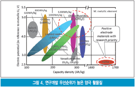
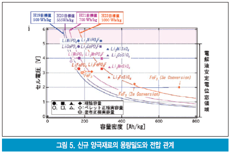
최근의 새로운 움직임으로서 Li2MO3(M: Ni, Co, Mn, Fe 등 천이금속)으로 조성을 나타내는 재료연구가 활발하다. 이들 재료는 방전용량이 250mAh/g로 매우 큰 것 등의 빼어난 성능을 보이는 것들이 보고되고 있다. 그림 5는 새로운 양극재료의 용량밀도와 전압과의 관계를 상세하게 나타내고 있다.
현재 널리 사용되고 있는 유기용매 전해질의 안전 전위창 영역에 속하는 신규 양극재료로는 Li2MPO4F와 Li2MSiO4(M: Ni, Co, Mn, Fe 등의 천이금속)과 다전자 반응을 보이는 FeF3 불화물 등이 있다.


▶ xLi2Mn2O3/(1-x)LiMO2(M: Li, Ni, Co, Al, Mg 등의 천이금속)계 재료 개발
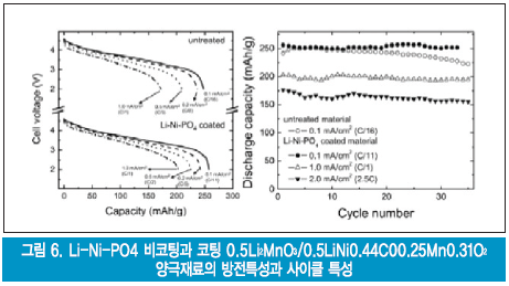
층상 구조의 양극소재는 3.0V보다 높은 전압에서 280mAh/g의 높은 이론 방전용량을 갖는다. 그러나 높은 산화특성과 구조적인 취약성 때문에 이러한 방전용량을 얻기가 힘들고 산소를 방출하기 때문에 전해액과의 발열반응 등이 발생한다. LiMn2O4 등의 스피넬 구조를 갖는 양극소재는 고 전위상태와 실온 이상의 고온에서는 Mn 이온이 전해액 속으로 녹아 나오는 특성이 있어 전기화학적으로 불안정하다는 약점을 가지고 있다. 이 때문에 온도 상승에 따라 용량 감소경향을 보인다. 또한 리튬이온이 모두 빠져 나간 상태에서는 강한 산화제인 MnO2가 형성되며, 이는 전해액을 산화시킨다. 이 약점을 보완하기 위하여 고용체인 xLi2Mn2O3/(1-x)LiMO2가 개발되었다.
xLi2Mn2O3/(1-x)LiMO2의 구조를 갖는 양극재료에서는 충전 시에 층상 구조의 LiMO2 부분으로부터 리튬이온의 탈리에서 발생하는 구조적인 불안정성을 Li2Mn2O3으로부터 리튬이온을 공급함으로서 산소 배열의 구조적인 안정성을 확보하는 역할을 한다. 이상적인 경우에는 LiMO2 → MO2 + Li+ + e- 과 Li2MnO3 → MnO2 + 2Li+ + 1/2O2 + 2e- 의 전기화학적 반응이 4.6V에서 일어난다. Li2MnO3으로부터 리튬과 산소가 탈리되나 MnO2는 원래의 상태로 머물게 된다.
M이 Co나 Ni인 경우 강한 산화제인 MO2와 MnO2는 입자표면에서 산소의 이탈이 발생하여 전극표면을 손상시키고 전해질의 산화를 촉진한다. 이는 용량 감소와 사이클 수명의 단축을 초래한다.

▶ Li2MO3계 재료 개발
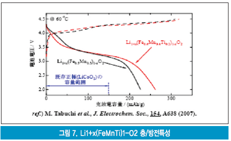
최근에는 리튬을 2개 갖는 재료 Li2MO3(M은 한 종류 또는 복수 종류의 천이금속 이온)의 조성으로 표현할 수 있는 재료연구가 수행되고 있다. C.S. Johnson 등은 이들의 방전용량이 250mAh/g로서 매우 크고 우수한 성능을 나타내는 것으로 보고 하고 있다. Li1-x(Fe0.4Mn0.4C00.2)1-xO2에서 초기 방전용량 226mAh/g을 개발하여 가능성 있는 새로운 양극재료를 찾아냈다. 이들은 고용량이며 가격 저감 가능성을 지녔으나 사이클 수명과 저온에서의 용량 저하 과제를 극복해야 한다. M Tabuchi 그룹은 Co를 Ti로 치환하여 그림 7과 같은 262mAh/g의 고용량의 양극재료를 개발하였다.


▶ LiMPO4(Fe, Mn, Ni, Mg, Co 등 천이금속)계 재료 개발
결정구조가 매우 안정하여 충/방전 특성이 우수한 Olivine 구조의 LiFePO4가 양극재료로 양산되고 있다. 그러나 작동전압이 3.4V로 상대적으로 낮아 에너지밀도가 낮다는 결점과 전기전도도가 매우 낮아 실용화에 어려움이 많았으나 나노화와 탄소 코팅기술의 개발로 실용화 수준에 도달하였다. Fe를 Mn으로 치환한 LiMnPO4는 LiFePO4와 같은 171mAh/g의 전류용량을 가지면서 작동전압은 4.0~4.1V로 높아 차량 탑재용으로 기대를 받고 있어 여러 곳에서 개발하고 있었다.
sol-gel법, poly-ole 공정, 수열합성법, 고상반응법, 최근의 마이크로파 가열 등 여러 공정으로 합성이 시도되었다. sol-gel법과 poly-ole 공정은 적절한 전지성능을 보이나 합성공정이 복잡하여 실용화의 가능성이 낮고, 수열합성법, 고상반응법 및 마이크로파 가열법에 의하여 얻어진 재료는 이론치의 40~60% 정도의 성능밖에 얻지 못하고 있었다.
I. Taniguchi 그룹은 미량의 Mg를 첨가한 LiMn0.96Mg0.04PO4를 에어로졸 프로세스와 분체기술을 사용하여 나노 입자화하고 탄소와 복합화 함으로써 전하이동 저항을 저감시키며 리튬이온의 확산거리를 줄인 새로운 양극재료를 개발했다. 입자크기는 평균 99㎚, 작동전압은 4.9V로서 이론적인 에너지 용량의 약 90% 수준에 도달하였다. 에어로졸 공정과 분체기술: 원료 염 용액을 300~500℃의 비교적 저온에서 분무 열분해하여 목적물의 전구체를 얻고 이를 나노 입자화하여 탄소와 복합화한 후에 이를 소성하는 방법이다.


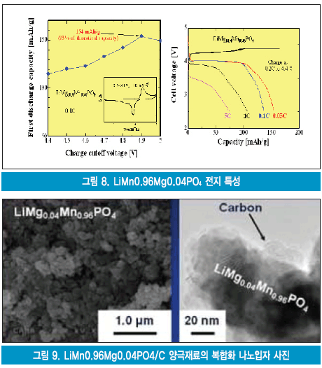
그림 8은 초기 충/방전효율과 cut-off voltage 및 충/방전특성이다. 그림 9는 LiMg0.04Mn0.96PO4/C 나노 컴복합화 입자상이다.

▶ FeF3계 재료 개발
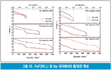
불화철(FeF3)은 LiFeF3의 리튬이온 삽입/탈리 반응인 Li++e-+FeF3 → LiFeF3에 의한 이론적 용량이 237mAh/g이지만 역반응 3Li++3e-+FeF3 → Fe+3LiF에서는 이론용량 711mAh/g, 에너지 밀도가 1400Wh/kg로서 대폭적인 용량 증대를 기대할 수 있다. 3전자 반응까지는 실용화가 어려울 것이나 2전자 반응까지는 리튬이온 삽입/탈리 반응을 실용화시킬 가능성이 보인다. 불화철 가격 등의 재료비는 약 1,700엔/kg으로 NEDO의 목표비용인 5,000엔/kg을 크게 밑돈다. 그림 10은 FeF3의 Li 및 Na 대극에서의 충/방전 특성을 보여준다.


FeF3와 아세틸렌 블랙(black)을 혼합한 시료에서는 340℃ 이상에서 발열 피크(peak)를 발견할 수 있었으나 그 밑의 온도에서는 발열 피크가 전혀 발생하지 않아 안정화되었다. 방전상태인 LiFeF3에서는 500℃까지 발열피크가 없어 열적으로 안정한 재료임을 확인하고 있다. MF3계인 FeF3, VF3, TF3의 열적 안전성을 시차주사열량계(DSC)로 측정한 결과, FeF3가 가장 발열량이 작았으며 일반적인 산화물 양극재료와는 달리 전해액 공존 하에서 전해액보다 발열량이 작아 안전성 관점에서도 매우 우수한 양극 소재임이 밝혀졌다. LiFeF3 양극을 사용한 laminate형 셀에서 130℃로 10분간 유지하는 Hot-box 시험과 못 박기 시험에서 파열·발화가 일어나지 않음을 확인했다.
▶ Li2MSiO4계 양극재료 개발
Li2MSiO4계 양극재료는 Li2Mn2 + SiO4 ↔ Mn4+SiO4 + 2Li+ + 2e- 전극반응에서 보듯이 2전자 반응이며 333mAh/g의 이론 용량을 보이는 매력적인 양극 활물질이다. 그러나 리튬이온의 탈리로 결정구조가 붕괴하여 반복적인 충/방전을 할 수 없다. M. Yasutomi 그룹은 Mn의 일부를 Fe로 치환하거나 SiO4의 일부를 PO4로 치환함으로써 반복 충/방전이 가능함을 밝혔다.
나. 음극재료 개발동향            


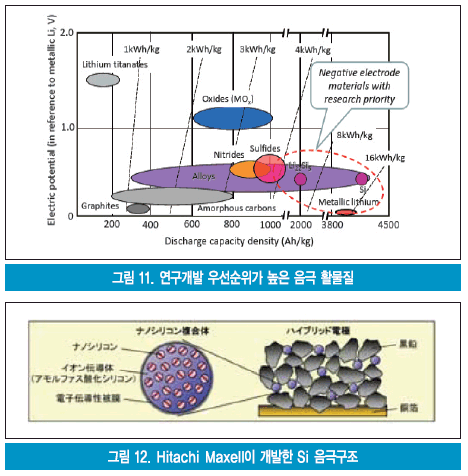
그림 11은 NEDO가 밝힌 음극재료 개발방향을 도식화 한 것이다. 흑연계 등은 전해액과의 반응성 억제, 합금과의 복합화기술에 의한 에너지밀도 향상 등이 개발방향이다. 2,500Wh/kg의 에너지밀도를 실현시킬 수 있는 SiO계, SnO계, 산화물계 재료의 실용화는 초기 불가역 용량의 저감과 신뢰성 향상 및 전해액과의 반응성 억제가 개발방향이다. 4,000Wh/kg의 에너지밀도를 실현할 수 있는 Si계, Sn계 등의 합금계 재료는 추가적인 장수명화와 신뢰성 및 열적 안전성 향상이 개발과제이다.
휴대형 전자기기용으로는 고용량의 연한 탄소(soft carbon)가 널리 사용되었으나 충전 말기에 리튬 덴드라이트(dendrite) 석출이 일어나 분리막 관통의 위험이 있어 EV용 등에서는 용량이 작아지지만 충/방전특성이 약간 향상되는 저 결정성의 경한탄소(hard varbon)이 널리 이용되고 있다.
흑연계 재료의 2배 이상의 고용량화가 가능하고 급속 충/방전특성이 우수한 실리콘계와 주석계 등의 합금계 음극도 나노화 기술과 박막화 기술로서 개발되고 있다. Sony는 비정질 SnCo/탄소음극을 사용하여 30%의 용량 향상과 -20℃에서의 방전용량을 40% 향상시켰다. Hitachi Maxell은 나노 실리콘 복합화/흑연음극의 상품화를 2010년으로 예정하고 있다. 그림 12는 Hitachi가 개발한 하이브리드 음극의 개념도이다.


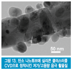
Panasonic은 실리콘 음극을 사용하여 용량을 30% 향상시킨 18650형 원통형 4Ah 리튬이온 이차전지의 양산을 2012년에 개시하여 휴대형 전자기기뿐만 아니라 가정용, 자동차용으로도 판매할 계획이다. P. Kumta는 석영기판 위에 탄소 나노튜브를 화학기상도금법(CVD: Chemical Vapor Deposition)으로 성장시킨 뒤에 CNT 위에 다시 CVD법으로 실리콘 나노 클러스터를 형성시켰는데, 그림 13는 음극 활성물질의 투과전자현미경 사진이다.
2.5C의 충/방전에서 1,000mAh/g의 에너지용량을 보였으며 99.9%의 쿨롱(coulomb) 효율을 보였다. 또한 리튬이온의 흡착/탈리에 수반되는 체적 팽창과 수축을 효과적으로 수용하고 있어 사이클 수명의 향상을 확인하였다.
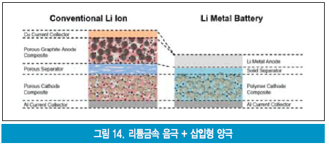
다. 리튬금속 음극의 사용 시도      
이론적 에너지밀도에서 가장 큰 값을 보이는 리튬금속(15,000Wh/kg, 8,000Wh/L)을 음극으로 사용하기 위해 덴드라이트 생성 억제, 장수명, 신뢰성 향상을 목적으로 한 기초적인 연구가 진행 중에 있다. 이들 기술 개발과제를 동시에 해결할 것으로 기대되고 있는 기술 중 하나가 전해질로 고체전해질을 사용하는 전고체 리튬이온 이차전지이다. 그림 14는 종래의 리튬이온 이차전지와 리튬금속/고체전해질을 사용하였을 경우의 에너지밀도 변화를 도식적으로 표시한 것이며, 성능이 크게 향상됨을 알 수 있다.


2012-02-25

No.8

           Bước tiến  mới với việc confirm lại vụ hierarchical ZnO nanorods mọc trên SnO nanofibers khá thành công. Tuy nhiên vẫn còn có một số các khuyết điểm là mọc vẫn chưa đồng đều. Mình đang tính ém cái vụ này, khi nào hoàn thành nốt thì tung ra cho ông thầy. Đảm bảo với ý tưởng check một hai khí hoặc tính chất quang của vật liệu composite này cũng đuợc vài topic nhỏ nhỏ hoặc to to.

Bứớc tiếp theo có thể gọi là kiếm khí và kiểm tra lại mấy cái Pt & Au substrates để tạo mẫu cuối cùng, công đoạn cuối cùng. Mịe, cái đế truớc thằng Hàn mang về to quá, khi mang lên Daejeon để check thì không vừa, nên là lại phải làm lại cái đế khác và mẫu khác. Đến là mệt.

Hôm qua ông thầy gọi điện tâm sự với mình những nửa tiếng lận, bàn đi bàn lại cái vụ chế tạo LiMn2O4 nanofibers. Bảo rằng làm mẫu nhanh nhanh lấy mấy gam để gửi đi chỗ khác làm pin và check hộ mình tính chất cuối cùng. Mấy cái khác cũng confirm lại rồi.
asspun nanofibers
và sau khi nung ở 500 độ C thì nó ra như vầy
Nói chung là cũng tàm tạm. Cố gắng đẩy nhanh tiến độ, sang tuần có đống mẫu cho ổng, rồi để mà còn viết abstract nữa chứ. haizzz
Cố lên nào....^.^ 


2012-02-19

No.6


Khó khăn …

Lâu rồi, từ khi mà một tháng trước quay trở về Việt nam, đến hôm nay mới có dịp thảo luận với tay Trung quốc về việc thực nghiệm được một chút. Hắn đang tổng hợp SnO2 cấu trúc hollow nanofiber type. Việc phat hiện ra cấu trúc này cũng là một sự tình cờ vào tầm khoảng tháng 10-11 năm ngoái sau khi giấc mơ theo đuổi làm LiFePO4 không thành công (sẽ bàn về sau). 1, 2 lần đầu khi phát hiện ra cấu trúc này. Ông thầy đã rất vui, chém gió bảo rằng mày có thể public lên bài tầm 8 hoặc 9 điểm. Và điều này khiến cho càng có động lực để nhanh chóng kêt thúc việc làm Postdoc ở đây. Nhưng, sau khi chuyển qua và tập trung nghiên cứu vấn đề  chế tạo nanofibers bằng electrospinning này đã gặp phải một số khó khăn. Mà khó khăn đầu tiên đó là làm sao để ổn định được hay xác định chính xác điều kiện tạo hollow type bởi vì khi lặp lại tương tự quá trình đó, dung dịch không đổi, điện thế và các tính chất điều khiển như dòng, độ nhớt dung dịch, kích thước của needle , khoảng cách giữa collector và needle. Đấy là chưa kể tới môi trường khi fibers tạo thành ra bên ngoài.

                                                  SnO2 hollow nanofibers

         Một phát hiện nữa là, trong quá trình pha chế dung dịch, SnCl2 , PVP hòa tan vào DMF sau đó rửa bằng nước thường thì thấy tạo kêt tủa trắng. Phân tích cho thấy kêt tủa trắng đó là SnO2. Và sau khi thảo luận với mình, hắn đã tập trung vào việc ổn định humidity-tức độ ẩm của không khí bên ngoài tác động vào. Việc điều khiển độ ẩm cực kì khó, bằng những cách thô sơ đơn giản không thể làm ổn định được. Cần phải có thiết bị, phải có máy móc. Tất nhiên nói tới việc mua thì càng khó khăn hơn nữa. Ông thầy cứ lắc đầu quầy quậy cho rằng chưa tối ưu và bắt phải giải quyết được triệt để trong điều kiện không mua thiết bị. Điều này khiến cho việc thực nghiệm kéo dài và hắn chán nản. Để làm được một mẫu cần phải mất khá nhiều thời gian. Ít nhất tầm 3 đến 4 ngày vừa làm, vừa chờ đợi. Lab lại chỉ có 2 máy electrospinning nên khá khó để chia sẻ cho từng thằng làm một trong khi có những 4 thằng tập trung vào chế tạo fibers. Có những lí do mà thầy không nói với trò về việc chịu chi hầu bao ra để mua thiết bị thực nghiệm đó là không nhiều các project và không nhiều tiền để mua các thiết bị máy móc cũng như hóa chất. Anh em làm việc cũng khó khăn vì ý tưởng. Nếu không mua được nhiều hóa chất, có nghĩa là làm việc và các ý tưởng bị cầm chừng. Thảo nào thằng trưởng lab suốt ngày quẩn quanh mấy cái topic về TiO2 ứng dụng cho DSSCs mà không có phát kiến gì gọi là đáng kể cả.
       Vấn đề 2 đó là sensor. Để make được 1 gas sensor nhất thiết phải có substrate. Vấn đề mang tính chiến lược và cốt lõi đó. Hiện tại không có nhiều công ti tham gia vào lĩnh vực đầy tiềm năng này. Đó là chế tạo các sub. Mỗi lần chế tạo đều phải đòi hỏi dùng Pt hay Au làm vật liệu đế. Mà giá cả của Platinum và gold thì biết rồi đấy. Thuộc vào hàng cực đắt nên rât ít những nơi có thể đăt mua được nó. Vì thế nó sẽ đẩy giá của 1 substrate lên tầm khoảng 300-500$ chưa tính các chi phí khác. Để kiếm được 1 sub hay ra quyết định mua nó tại thời điểm hiện tại là khá khó đối với ông thầy. Cả thầy và trò đều muốn đăng paper nhưng việc quan trọng là thầy có chịu chi hay không. Lĩnh vực sale sub này có vẻ nhiều tiềm năng, liên quan tới kinh tế khá mở và hi vọng sẽ tóm lấy cơ hội này để kinh doanh phát nhể ?

No.5


Nanobarbed fibers : Cấu trúc nano cho vật liệu tiên tiến

           Về mặt ý tưởng mà nói thì ZnO được nghiên cứu từ khá lâu vì giá thành rẻ, nhiều ứng dụng trong các lĩnh vực khác nhau. Có thể thay thế cho TiO2 với bề rộng vùng cấm tương đương nhau (3.3~3.4 eV) và điều kiện chế tạo khá ổn định. TiO2 khó chế tạo hơn vì có 2 dạng cấu trúc riêng ZnO cấu trúc tinh thể chỉ có 1 là dạng cấu trúc lục giác. Vì thế cho nên hiện tại ZnO vẫn đang là một đề tài hot, mặc dù có quá nhiều những public paper về vấn đề này. Chính vì lẽ đó để tìm được một ý tưởng mới, xây dựng một cấu trúc mới với hệ vật liệu ZnO thì khá khó khăn.Nhưng cũng không phải là không có cách.
Lab tôi, mà chủ trương của thầy là xây dựng dạng rod mọc trên fiber. Và thu được khá thành công với 2 vật liệu ZnO và TiO2
-> TiO2 NBFs (published on App.Phys)


-> ZnO NBFs (Published on App.Phys )

Cấu trúc này cũng có sự tiến bộ hơn  những hệ cấu trúc khác đó là diện tich mề mặt lớn, tăng được diện tích bề mặt theo thời gian mọc nanorods. Có những ứng dụng trong làm vật liệu photocatalytic, gas sensors và solar cells. Nhưng cũng có những disadvantage đó là tiếp xúc giữa vật liệu và đế rất ít, khó khăn với chế tạo khối lượng lớn.
Gần đây có phát triển nghiên cứu với SnO2 NBFs nhưng điều này khá khó khăn. Mà có thể nói gần như là không thể. Một số rất ít các public paper  chạy theo xu hướng nghiên cứu về mảng cấu trúc này. Rộng ra có thể xây dựng được cấu trúc với nhiều loại bán dẫn, phi dẫn hoặc oxide kim loại khác...

2012-02-15

No.3


A study on the physical and electrochemical properties of
V2O5 nanofibers synthesized by electrospinning

De Pham-Cong1, Kyun Ahn1, Fukai Shan1, Ha-Anh Dao2,Chae-Ryong Cho*

1Department of Nano Fusion Technology, Pusan National University, Miryang 607-706
2 Pohang University of Science and Technology, Pohang, Gyongsangbuk-do 791-708


Abstract
            
Vanadium pentoxide (V2O5) nanofibers have interesting as materials of electrode for lithium ion batteries. In this study, we present the physical and electrochemical properties of V2O5 nanofibers synthesized by using electrospinning method. To fabricate V2O5 nanofibers, solution is consists of vanadium acetylacetonate as sol and  Polyvinypyrolydone gel. After fabricate V2O5 nanofibers, annealing process was conducted at 500oC to make only pure V2O5 nanofibers. The surface morphology and structure were measured by field emission scanning electron microscope (FE-SEM), x-ray diffraction (XRD) and Raman spectroscopy. From the analysis of FE-SEM, XRD and Raman spectra on V2O5 nanofiber, the diameter and crystal structure of V2O5 nanofibers were measured 100~200 nm with polycrystal structure. And the surface area of V2O5 nanofiber was measured by  Brunauer Emmett Teller (BET). Electrochemical properties of the synthesized products as electrodes in capacitor device were also studied using cyclic voltammetry.


Keywords: electrospinning, V2O5, cyclic voltametry 

No.2


Effect of reactive gas in an atmospheric plasma
for dye adsorption on ZnO nanorods

De PHAM-CONG, Kyun AHN, Jong-Man KIM,
Se-Young JEONG and Chae-Ryong CHO*
College of Nanoscience and Nanotechnology, Pusan National University, Busan 609-735

Jong Pil KIM and Hyun Gyu KIM
Busan Center, Korea Basic Science Institute, Busan 609-735

Hyung Soo AHN and Hong Seung KIM
Department of Applied Science, Korea Maritime University, Busan 606-791

In this study, ZnO nanorods (NRs) were grown on F-doped SnO2 (FTO)/glass substrate by using a chemical bath deposition (CBD) method. The NRs were crystallized well. The surfaces of the NRs were modified using an atmospheric-pressure (AP) plasma containing reactive gases such as O2, H2, and N2. In the case of the Ar/O2 and Ar/N2 plasma-treated ZnO NRs, chemical bonding states and the dye adsorption on the surface of the ZnO layer increased because of –O and –OH radicals. We present the efficiencies of ZnO-NR-based dye-sensitized solar cells (DSSCs) treated with AP plasmas containing reactive gases.

PACS number: 68.35.Md, 68.43.Mn, 52.75.-d, 79.60.-i
 Keywords: Surface energy, Plasma, Hydroxyl bonds, Dye adsorption
*Corresponding author; E-mail: crcho@pusan.ac.kr


I. INTRODUCTION
Photovoltaic devices generate clean energy that can reduce the world’s dependence on conventional energy sources. Dye-sensitized solar cell (DSSCs) might be the most efficient and stable excitonic photocells [1, 2]. DSSCs with a metal oxide nanostructure have been studied as a low-cost alternative to silicon because of the simple manufacturing process, large-scale production capability, and potential applications as semiconductor-based p-n junction solar cells [3, 4]. Recently, ZnO was used as a candidate material for replacing TiO2 because the energy-band structure of ZnO with a wide band gap (3.37eV) and its physical properties are similar to the energy-band structure and physical properties of TiO2. Furthermore, ZnO has higher electronic mobility, which would be remarkable for electron transport (a high exciton binding energy of 60 meV), with possible reduced recombination loss [5].
In particular, the synthesis of one-dimensional nanostructures of ZnO, replacing the existing nanoparticle structure, is attracting a lot of interest owing to their unique properties and integration into DSSCs [6]. On the other hand, the increase in efficiency achieved using ZnO-based DSSCs has been limited because of the generation of the Zn2+/dye complex at the interface between ZnO and dye. ZnO is immersed in a solution of sensitizer dyes, and a small amount of Zn2+ ions from the ZnO surface are dissolved in the solution. During the process, a Zn2+/dye complex is formed on the ZnO surface. Among several dyes, N719 dye with two carboxyl groups having very low acidity is used to reduce the formation of a Zn2+/N719 dye complex on the surface of ZnO [7]. To increase dye adsorption, recent research has focused on the production of –O and –OH radicals on the surface of the ZnO layer by using physical and chemical treatment [8-10]. Among the various techniques for surface modification, plasma treatment is a simple, low-cost, and mass-production method, however, the effect of an atmospheric-pressure (AP)  plasma on solar cell efficiency has not been reported.
In this article, we report the growth of ZnO nanorods (NRs) achieved using a chemical bath deposition (CBD) method. For surface modification, the grown ZnO NRs were annealed and treated with an AP plasma containing the reactive gases Ar/O2, Ar/N2, and Ar/H2. The crystal structures, morphologies and surface chemical bonding states of the ZnO NRs were investigated. In this paper, the results for the dye adsorption and the efficiency of the ZnO NRs-based DSSCs are discussed for the first time.
                                                                            
II. EXPERIMENTS AND DISCUSSION
ZnO thin films were deposited on a F-doped SnO2 (FTO)/glass substrates by RF magnetron sputtering. For growing ZnO NRs, 400 ml of an aqueous solution containing 0.03-M zinc acetate dehydrate (ZnAc) [Zn(O2CCH3)2(H2O)2, 98% purity] and 0.03-M hexamethylenetetramine (HMT)  [(CH2)6N4, 99% purity] as a precursor was prepared at room temperature. The substrate was immersed at the bottom of the beaker containing the prepared aqueous solution, and the beaker was maintained at 92°C for 2.5 h for the growth of ZnO on the substrate. The substrate was reversed during the growth process. After the completion of the growth process, the NRs were rinsed with deionized water and dried in air to remove any residual salt and organic materials (U-ZnO).  After the NRs had been grown for 10 h, they were annealed at 400°C for 2 h (A-ZnO) and were treated with an AP plasma (FemtoScience, PlasmafluxTM) containing O2, N2 and H2 gases at a RF power of 100 W for 30 min (O-ZnO, N-ZnO and H-ZnO). The flow rate of Ar was 40 sccm, and that of each of the reactive gases, i.e., O2, N2, and H2 was 5 sccm. To examine their photovoltaic behavior, we immersed the ZnO NRs in a solution of cis-bis(isothiocyanato)bis(2,2’-bipyridyl-4,4’dicarboxylato)-ruthenium(II)bis tetrabuthylammonium dye (N719, Solaronix) for 24 h at room temperature. A dye-adsorbed ZnO electrode was assembled with a Pt counter electrode to form a DSSC. One drop of an electrolyte solution (Iodolyte AG-50, Solaronix) was infiltrated between the two electrodes. The physicochemical properties of the ZnO NRs were investigated using field emission scanning electron microscopy (FESEM) (S-4700, Hitachi), X-ray diffractometry (XRD) (X’pert pro, Phillips), and X-ray photoelectron spectroscopy (XPS) (ESCALAB250, VG Scientific). The dye adsorption of the NRs was measured using a UV-VIS-NIR spectrophotometer (Cary 5000, Varian). The current density-voltage (J-V) characteristics of cells with active areas of 0.25 cm2 were measured using an AM 1.5 solar simulator fitted with a Xe lamp.
Figure 1 shows SEM images of the ZnO NRs grown on ZnO/FTO/glass. The ZnO NRs had a hexagonal shape and were arranged in a vertical array in the [001] direction on the ZnO seed layer. After a few minutes, the NRs nucleated on the seeds in the ZnO thin layer. The diameters of these NRs were significantly larger than those of the ZnO nanoparticle seeds in a thin film. In the initial reaction step, after 2.5 h, the growth of ZnO NRs stopped, and their average length and diameter were approximately 1.75 μm and 76 nm, respectively (Fig. 1(a)). The length and the diameter of the NRs increased with increasing duration of the repeated reaction (5, 7.5, and 10 h) at the same precursor concentration, as shown in Figs. 1(b-d). The average length and diameter of the NRs after 10 h were approximately 3.8 μm and 150 nm, respectively. Moreover, the NR diameter increased steadily during the growth period, but at a much slower rate than the NR length. The growth rate of the ZnO NRs in the vertical direction was very fast during the initial reaction; however, the rate reduced with increasing reaction time because of an increase in NR growth in the radial direction. Figure 1(e) shows the morphology of A-ZnO NRs that were annealed to remove any residual organics material and to increase the crystallinity. The shapes of the AP-plasma-treated O-ZnO, N-ZnO and H-ZnO NR samples did not show any significant changes (Figs. 1(f-h)).
Structural analyses of the NR samples grown on ZnO/FTO/glass for various reaction times and annealed and treated with Ar/O2, Ar/N2 and Ar/H2 AP plasma (shown in Fig. 2) were carried out using XRD. For the ZnO NRs with a hexagonal wurtzite structure, the (002) peak was dominant, and the peak intensity increased with increasing duration of the repeated reaction because of NR growth in the [002] direction, as shown in Figs. 2(b-d). The (002)/(101) peak height ratio increased with time because only those NRs that had a c-axis almost normal to the substrate, NRs that contributed to the (002) diffraction peak, continued to grow. The peak intensity corresponding to A-ZnO NR was much higher than that corresponding to U-ZnO NRs (Fig. 2(e)). This phenomenon was attributed to the removal of residual organic molecules and an increase in crystallinity, resulting from the arrangement of interior lattices. On the other hand, there were no significant changes in the peak intensities corresponding to the O-ZnO, N-ZnO and H-ZnO NRs samples.
   XPS was used to obtain more information about the surfaces of the ZnO NRs. Figure 3 shows the surface chemical bonding states in the Zn 2p and O 1s XPS spectra. Figure 3(a) shows the O 1s XPS spectra deconvoluted using a Gaussian-Lorentz fit. Herein, the peak at the binding energy of 530.1 eV corresponds to the Zn-O bond in the wurtzite structure. The peak at 531.5 eV was assigned to the -OH bond in zinc oxyhydroxide species with an oxygen-deficient region in the ZnO matrix. The binding energy of 532.3 eV was attributed to weakly bound oxygen, such as the oxygen in adsorbed H2O and O2 [11]. The Zn 2p spectra show a doublet peak at binding energies of 1021.2 eV and 1044.3 eV corresponding to the Zn 2p3/2 and Zn 2p1/2 core levels, respectively (Fig. 3(b)) [12]. The increase in the Zn 2p peak area of the treated ZnO NRs was greater than that for the U-ZnO NRs but there was no change in the peak area ratios of Zn 2p3/2 to Zn 2p1/2.
Figure 4 shows the absorption spectra and the J-V curves for the N719-sensitized ZnO-NR-based DSSCs. A broad absorption band peaking at 520 nm can be observed, which was assigned to the metal-to-ligand charge-transfer transition (MLCT) of N719 [13-15]. The dyes was adsorbed on the ZnO NRs after the formation of H2O in chemical reactions involving -O, -OH radicals on the surface of the ZnO NRs and -COOH radical in the dye molecules [16, 17]. The absorption intensity for A-ZnO NRs was similar to that for U-ZnO NRs because of a decrease in the concentration of the -OH radical and an increase in the concentration of the -O radical. Furthermore, dye adsorption of O-ZnO and N-ZnO NRs increased when -OH radicals were added during the Ar/O2, and the Ar/N2 AP-plasma treatments. Therefore, the intensity of this band, which is a characteristic of dye adsorption, increased with increasing concentration of A-ZnO, O-ZnO and N-ZnO NRs. In particular, O-ZnO NRs showed the highest dye adsorption because the increase in the concentration of the -OH radical was more than that for N-ZnO NRs. On the other hand, H-ZnO NRs showed less dye adsorption than A-ZnO NRs because of a significantly decreased concentration of -O radicals on the NR surface.
The open-circuit voltage (Voc) of the U-ZnO was 0.63 V, but those for the A-ZnO, O-ZnO, N-ZnO, and H-ZnO NRs were 0.71, 0.81, 0.80, and 0.80 V, respectively. The value of Voc for U-ZnO NRs was less than those for A-ZnO NRs and plasma-treated ZnO NRs because of the presence of a relatively large amount of residual organic molecules on the surfaces of the ZnO NRs. The short-circuit current density (Jsc) of the U-ZnO NRs (1.76 mA/cm2) was smaller than those for the A-ZnO NRs (2.41 mA/cm2), O-ZnO NRs (3.37 mA/cm2), N-ZnO NRs (2.72 mA/cm2) and H-ZnO NRs (2.18 mA/cm2). In particular, the value of Jsc was highest for O-ZnO NRs and was relatively low for H-ZnO NRs as compared to N-ZnO and A-ZnO NRs. Consequently, the PV efficiency of O-ZnO NRs (1.21%) was higher than those of U-ZnO NRs (0.51%), A-ZnO NRs (0.83%), N-ZnO NRs (0.99%), and H-ZnO NRs (0.79%). The significant change in the cell efficiencies of O-ZnO NRs and N-ZnO NRs based DSSCs might be due to the analysis and measurement conditions. The XPS data were generally measured for a few top NR layers instead of the sidewalls of the NRs. On the other hand, the plasma affects the entire sample. The effect of annealing and O2-AP-plasma treatment in series increased the PV efficiency to 62% and 137% more than that of the untreated samples, respectively.

III. CONCLUSION
The grown ZnO NRs were oriented along the [001] direction and had a hexagonal wurtzite structure. The shape of the NRs was determined and the length of the NRs were observed to increase with increasing reaction time. There were no significant changes in the morphologies and structures of A-ZnO, O-ZnO, N-ZnO and H-ZnO NRs after the annealing and plasma-treatment. The concentrations of -O and -OH radicals in A-ZnO, O-ZnO, and N-ZnO NRs increased because of the supply of these polar groups (-O and -OH) produced in AP plasmas containing reactive gases. O-ZnO NRs showed the highest level of dye absorption because of the largest polar components. Consequently, O-ZnO-NR-based DSSCs showed higher efficiency (1.21%) than the other DSSC samples because of the increased crystallinity and dye adsorption. Our results support the fundamental insights for enhancing the efficiency of nanostructure based DSSCs by treating them with AP plasmas containing reactive gases.

ACKNOWLEDGMENT
This study was supported by a Korea Research Foundation Grant (KRF-2008-313-D00607).

REFERENCES
[1]    M. K. Nazeeruddin, P. Pechy and T. J. Renouard, J. Am. Chem. Soc. 123, 1613 (2001).
[2]    P. Wang, M. S. Zakeeruddin, J. E. Moser, K. M. Nazeeruddin, S. Takashi and M. Graetzel, Nature Mater. 2, 402 (2003).
[3]    M. K. Nazeeruddin, F. D. Angelis, S. Fantacci, A. Selloni, G. Viscardi, P. Liska, S. Ito, B. Takeru and M. Grätzel, J. Am. Chem. Soc. 127, 16835 (2005).
[4]    G. Oskam, Z. S. Hu, R. L. Penn, N. Pesika and P. C. Searson, Phys. Rev. E 66, 011403 (2002).
[5]    Q. Zhang, C. S. Dandeneau, X. Zhou, and G. Cao, Adv. Mater. 21, 4087 (2009).
[6]    H. Horiuchi, R. Katoh, K. Hara, M. Yanagida, S. Murata, H. Arakawa and M. Tachiya, J. Phys. Chem. B 107, 2570 (2003).
[7]    F. Yan, L. Huang, J. Zheng, J. Huang, Z. Lin, F. Huang and M. Wei, Langmuir 26, 7153 (2010).
[8]    J. Chung, J. Lee and S. Lim, Physica B 405, 2593 (2010).
[9]    S. K. Park, C. Kim, J. H. Kim, J. Y. Bae and Y. S. Han, Curr. App. Phys. 11, 131 (2011).
[10] C. Kim, J. T. Kim, H. Kim, S. H. Park, K. C. Son and Y. S. Han, Curr. App. Phys. 10, 176 (2010).
[11] X. G. Han, H. Z. He, Q. Kuang, X. Zhou, X. H. Zhang, T. Xu, Z. X. Xie and L. S.
Zheng, J. Phys. Chem. C 113, 584 (2009).
[12] N. S. Ramgir, D. J. Late, A. B. Bhise, M. A. More, I. S. Mulla, D. S. Joag and K.
Vijayamohanan, J. Phys. Chem. B 110, 18236 (2006).
[13] N. Chantarat, Y. W. Chen, S. Y. Chen and C. C. Lin, Nanotechnology 20, 395201
(2009).
[14] G. Benkö, J. Kallioinen, J. E. I. Korppi-Tommola, A. P. Yartsev and V. Sundström, J.
Am. Chem. Soc. 124, 489 (2002).
[15] Y. Zhang, Z. B. Xie and J. Wang, Nanotechnology 20, 505602 (2009).
[16] K. Ahn, Y. S. Jeong, H. U. Lee, S. Y. Jeong, H. S. Ahn, H. S. Kim, S. G. Yoon and C.
R. Cho, Thin Solid Films 518, 4066 (2010).
[17] F. M. Fowkes, J. Phys. Chem. 382 (1962).